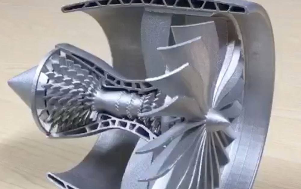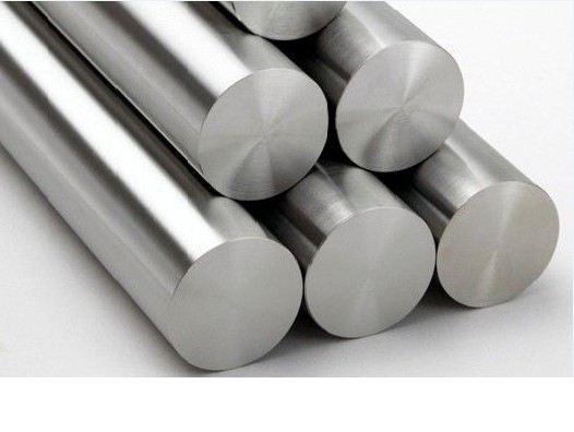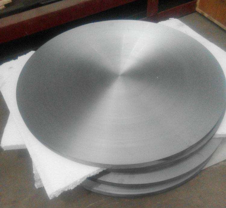
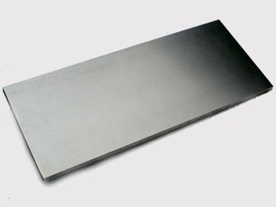
Molybdenum alloy target
The coating target is a sputtering source for forming various functional films on the substrate by sputtering under appropriate process conditions by magnetron sputtering, multi-arc ion plating or other types of coating systems. To put it simply, the target is the target material for high-speed energy-energy particle bombardment. It is used in high-energy laser weapons. When different power densities, different output waveforms, and different wavelengths of lasers interact with different targets, different damage will occur. effect. For example, the evaporation magnetron sputtering coating is a heating evaporation coating, an aluminum film, or the like. Different film materials (such as aluminum, copper, stainless steel, titanium, nickel targets, etc.) can be obtained to obtain different film systems (such as super hard, wear-resistant, anti-corrosive alloy films, etc.).
Craftsmanship
Magnetron sputtering target
1) Principle of magnetron sputtering:
An orthogonal magnetic field and an electric field are applied between the sputtered target (cathode) and the anode, and the required inert gas (usually Ar gas) is charged in the high vacuum chamber, and the magnet forms 250-350 Gauss on the surface of the target material. The magnetic field, together with the high voltage electric field, constitutes an orthogonal electromagnetic field. Under the action of electric field, Ar gas is ionized into positive ions and electrons, and a certain negative high voltage is applied to the target. The electrons emitted from the target are affected by the magnetic field and the ionization probability of the working gas increases, forming a high-density plasma near the cathode. Body, Ar ion accelerates to the target surface under the action of Lorentz force, bombards the target surface at a high speed, so that the sputtered atoms on the target follow the momentum conversion principle and fly away from the target surface with higher kinetic energy. The substrate is deposited into a film. Magnetron sputtering is generally divided into two types: DC sputtering and RF sputtering. The principle of DC sputtering equipment is simple, and the rate is also fast when sputtering metal. The use of RF sputtering is more extensive. In addition to sputterable conductive materials, non-conductive materials can be sputtered, and reactive sputtering can also be used to prepare compound materials such as oxides, nitrides, and carbides. If the frequency of the radio frequency is increased, it becomes microwave plasma sputtering. Today, electron cyclotron resonance (ECR) type microwave plasma sputtering is commonly used.
2) Magnetron sputtering target types:
Metal sputter coating target, alloy sputter coating target, ceramic sputter coating target, boride ceramic sputtering target, carbide ceramic sputtering target, fluoride ceramic sputtering target, nitride ceramic sputtering Target, oxide ceramic target, selenide ceramic sputtering target, silicide ceramic sputtering target, sulfide ceramic sputtering target, germanide ceramic sputtering target, other ceramic targets, chromium-doped Silicon ceramic target (Cr-SiO), indium phosphide target (InP), lead arsenide target (PbAs), indium arsenide target (InAs).
Application field
It is well known that the technological development trend of target materials is closely related to the development trend of thin film technology in downstream application industries. As the application industry improves on thin film products or components, target technology should also change. Such as Ic manufacturer. Recently, we are working on the development of low-resistivity copper wiring. It is expected that the original aluminum film will be greatly replaced in the next few years, so the development of copper targets and their required barrier targets will be urgent. In addition, in recent years, flat panel displays (F P D) have largely replaced the market for computer monitors and televisions based on cathode ray tubes (CRTs). It will also significantly increase the technology and market demand for ITO targets. Also in terms of storage technology. Demand for high-density, high-capacity hard drives and high-density rewritable discs continues to increase. These have led to changes in the demand for targets in the application industry. Below we will introduce the main application areas of the target, as well as the trend of target development in these areas.
Microelectronics
In all application industries, the semiconductor industry's quality requirements for target sputtered films are the most demanding. Now 12-inch silicon wafers have been manufactured. The width of the interconnect is decreasing. Silicon wafer manufacturers' requirements for targets are large size, high purity, low segregation, and fine grain size, which requires the target to have a better microstructure. The crystal particle diameter and uniformity of the target have been considered to be the key factors affecting the film deposition rate. In addition, the purity of the film is highly dependent on the purity of the target. The past 99.995% (4 N5) purity of the copper target may meet the needs of the semiconductor manufacturer's 0.3 5pm process, but it cannot meet the current 0.2 5um process requirements. The 0.18um of the meter is even 0.13m, and the required target purity will be required to reach 5 or even 6N. Compared with copper, copper has higher resistance to electromigration and lower resistivity, which can be met! The need for sub-micron wiring with a conductor process below 0.25 um, but with other problems: the adhesion strength of copper to organic dielectric materials is low. And it is easy to react, resulting in the copper interconnect of the chip being corroded and broken during use. In order to solve the above problems, it is necessary to provide a barrier layer between the copper and the dielectric layer. The barrier layer material generally uses a metal having a high melting point and a high electrical resistivity and a compound thereof. Therefore, the thickness of the barrier layer is required to be less than 50 nm, and the adhesion property to the copper and the dielectric material is good. The barrier properties of copper interconnects and aluminum interconnects are different. There is a need to develop new target materials. The target for the barrier layer of the copper interconnect includes T a , W, T a S i , WS i , and the like . But T a and W are both refractory metals. Production is relatively difficult, and it is now being studied as a substitute for gold such as molybdenum and chromium.